This week we came across the news that Samsung will have to start paying for the use of FinFET technology . But does the term really mean the term?
For those who have some familiarity with electronic products, you have certainly come across the term FinFET. It is constantly present in technical specifications of processors, SSDs, tablet and mobile CPUs and still video cards.
What is FinFET?
FinFET is an acronym for “Fin Field Effect Transistor” (free-field transistor effect). The technology itself is considered simple, yet it is important to take some principles into account.

One of them says that inside any microchip, be it RAM, SSD or processor of various types, millions or billions of transistors can be found. These components are responsible for transforming electricity into data.
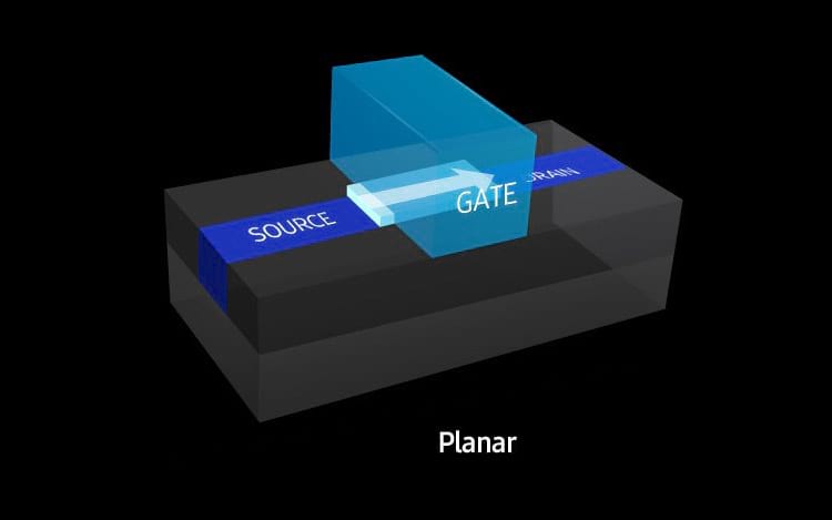
Thus, when a manufacturer speaks of processor from a manufacturing process, lithography or FinFET architecture is referring to an arrangement in which the transistors of the chip are organized into 3D structures, with stacking.
The FinFET transistors can have port thickness of 5 nanometers and width of 50 nm. FinFET technology is widely used by AMD, Nvidia, IBM, Samsung, Intel and Motorola.
Smaller chips every generation
With each generation, the scale of the chips tends to decrease. In summary, this is the most efficient method for producing better products. The smaller the distance between the terminals of the transistors that are inside the chip, the less distance the electricity needs to travel. This all makes data processing faster.
To complete, in this case, the electricity also finds less resistance for its passage. Another advantage of decreasing chip size is the area gain. Thus, if the distance between transistors is smaller, it is possible to include a few more million of them in the same space occupied by the previous generation processor. To top it all, overall, with shrinking architectures, manufacturing costs tend to decline.
In sum, the fundamental principles that command the semiconductor industry is the increase in performance and the decrease in consumption. The trend is that every year companies release new processors that meet the needs.

Future of FinFET
As we saw above, FinFET is the term for chips (processors, GPUs and SSDs) that use 3D transistors, with a design structure that looks like a fin.
The technology arose from the need to prevent the passage of electricity that was seen in the previous technology. Thus a three-dimensional transistor was developed. Instead of a flat, flattened 2D structure, a sort of fin was created to insert a physical barrier to the involuntary jumps of energy that were seen before, which prevented the leakage of current that could compromise the operation of the chip.
Intel was the forerunner of the technology, with its Tri-Gate Transistor, which debuted at the 2012 Ivy Bridge architecture, also called Intel’s third-generation processors, which is 22 nanometers versus the 32 nm Sandy Bridge, 2011 .
Brand technologies
Regarding the future, there is still no clear idea of what to actually do if silicon proves to be infeasible from a certain scale. Until then, the intention is to keep FinFET technology in use.
In summary, FinFet is the technology that has brought to the chips, a new organization of the transistors, making them smaller and more perfomous, however, there are physical barriers that we will certainly achieve. Only time will bring us a new technology that will be able to produce performance, consuming less space and energy.
